时间:2015年7月13-15日
地点:教十一413房间(四楼物理系会议室)
授课日程及授课人简历等详见后续介绍

Lecture schedule of advanced transmission electron microscopy by Prof. N. Tanaka
at Hangzhou
<July 13(Mon) morning, 9:30-12:00>
1. What is nano-word ?
2. What is transmission electron microscopy(TEM) ?
3. Basic principles of transmission electron microscopes
<July 13 (Mon) after noon 13:30-16:00>
4.Application of TEM to materials science, several examples
5.Electron guns, coherence of illumination, and diffraction physics.
<July 14(Tues), morning>
6. More advanced knowledge of HRTEM, particularly contrast transfer function
7. Aberration correction on TEM
<July 14 (Tues), afternoon>
8. What is scanning transmission electron microscopy(STEM)
9. Basic principles of STEM imaging and image calculation
10. Application of STEM to various specimens
<July 15(Wed), morning, 10:00-11:30.
Seminar on some topic on environmental transmission electron microscopy
<July 15(Wed), afternoon>
Discussion and seeing the university and others
 Curriculum Vitae
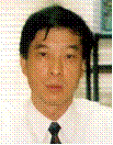
Nobuo Tanaka, Ph. D, Japanese.
Designated Professor of Ecotopia Science Institute,
Nagoya University, Chikusa-ku, Nagoya, 464-8603, Japan.
President of Japanese Society of Microscopy
Tel: +81-52-788-6261, Fax: +81-52-789-3827
Studies:
(1)Nano-structural science, Thin film physics, Catalysis science, and Surface physics. (2)High-resolution electron microscopy, Environmental electron microscopy,
Three-dimensional electron microscopy of small clusters, interfaces and surfaces.
(3)Study of magnetic properties of transition metal clusters and micro-devices studied
by spin-polarized electrons and vortex electron beams.
(4)Study of semiconductor interfaces by aberration corrected electron microscopy.
(5)Study of catalytic particles by in-situ electron microscopy.
(6)Study of nanowires and carbon nanotubes as well as fullerenes and graphenes
(7)Study of human-cells and polymers by 3D electron microscopy.
Appointed: (1)Committee member of electron diffraction
in international union of crystallography(IUCr).
(2)Chairman of the program committee of the IMC-16(2006, Sapporo).
(3)Program committee member of the IMC-17(2010, Rio de-Janeiro).
(3) Head of electron microscope laboratory in Nagoya University.
(4) Visiting professor of Helsinki Institute of Technology
Book authors:
(1)"Scanning Transmission Electron Microscopy for Nano-Materials"
(Imperial College Press, 2013)
(2)"Advances in Imaging and Electron Physics", Vol.153 (Academic Press,2008)
(3) "Denshisen-Nano-Imaging" (Uchida-Rokaku-Ho, 2009) <in Japanese>
(4)" Nano imaging" (NTS Press, 2008) , <in Japanese>
(5)"Physics and Chemistry of Clusters" (Kodansha-Scientific, 1997)
(6)"Metal-Semiconductor Interfaces" (Ohm-sha Press, 1995)
14 others
Scientific papers:
(1)N. Tanaka et al., "Development of an environmental high-voltage electron
microscopy for reaction science", Microscopy, 62(2013), 205-215.
(2)T. Fujita et al., "Atomic origins of high-catalytic activity of nano-porous gold, Nature
Materials, doi: 1-1038 (2012)
(3)M.Kuwahara et al., "30kV-spin polarized transmission electron microscope with
GaAs-GaAsP strained superlattice photocathode", Appl. Phys. Lett., 101(2012)
033102.
(4) K. Saitoh et al., "Measuring the orbital angular momentum of electron vortex
beams using a forked grating", Phys. Rev. Lett.,111(2013), 074801.
(5)J. Yamasaki et al., "Atomic structure analysis of stacking faults and misfit
dislocations at 3C-SiC/Si(001) by aberration-corrected transmission
electron microscopy", J. Phys. D, 45(2012), 494002.
more than 200 others.


