时间:7月2日(星期三)上午 9 : 30
地点:硅材料国家重点实验室1号楼会议室
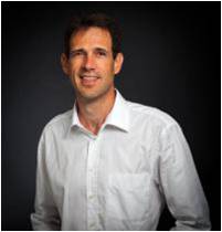
主讲人: Prof. Bruno Grandidier, IEMN, CNRS, France
邀请人:皮孝东
题目:Novel experimental schemes to study the impact of excited electrons on devices and nanomaterials
Abstract:In a wide range of semiconductor applications, the characterization of the local conductivity is crucial for the final device performance. To fulfill this goal, four-point probe measurements are relevant, due to the low requirements on sample preparation. But with the ongoing reduction in size of the devices, standard probes can become very invasive and the dominant source of scattering at the nanoscale. Therefore, the use of probes operated with a scanning tunneling microscope (STM) has considerable potential, as it does not need any extra electrodes on the specimen and enables arbitrary arrangements of probe electrodes with the highest spatial resolution. Based on the atomic precision of motion control of STM and, real-time and fast imaging capability of scanning electron microscopy (SEM), we will show how this instrument can be used to characterize
semiconductor materials and gives insight into the contribution of surface effects in their transport properties.
Carrier multiplication, the generation of an electron-hole pair from a hot electron, is of prime importance to master amplification phenomena in materials and multiply the output of opto-electronic devices and solar cells. As a result, the talk will first discuss the applicability of this technique for measuring the quantum yield of impact ionization. We will describe how electron and holes can be respectively measured, enabling the direct and unambiguous determination of the quantum yield. Thanks to the scanning ability of the STM tips, spatial mapping of the carrier multiplication efficiency will be achieved, giving access to the combined effect of impact ionization, carrier diffusion and recombination in Si p-n junctions at the nanoscale.

Prof Bruno Grandidier, Department of Physics, Institut of Microelectronics, Electronics and Nanotechnology Director of Research at CNRS (DR1, First Class). 1999-2001 : Assistant Professor of Physics, Institut Supérieur d’Electronique et du Numérique (ISEN) 2001-2010 : CNRS Research Scientist, Institut of Microelectronics, Electronics and Nanotechnology (IEMN) Since 2006 : Head of the research team “Physics of Nanostructures and Quantum Devices” at IEMN Since 2010 : Senior CNRS Research Scientist, Institut of Microelectronics, Electronics and Nanotechnology Since 2013 : Dean of Physics Faculty at the Institut Supérieur d’Electronique et du Numérique (ISEN)


